|
")
Graphene is a one-atom-thick planar sheet of bonded carbon atoms that are densely packed in a honeycomb crystal lattice. The carbon-carbon bond length in graphene is about 0.142 of a nanometer; the “sheet” itself can be visualized as atomic-scale chicken wire made of carbon atoms and their bonds. In recent years, researchers found that graphene has unique properties that make it an excellent material for semiconductors, along silicon.
Now, physicists at the University of California, Berkeley (UC Berkeley), and the Lawrence Berkeley National Laboratory (LBNL) have found that graphene can sprout nanobubbles in which electrons behave in a bizarre way, if it is stretched in a specific way. Specifically, the electrons within each nanobubble segregate into quantized energy levels instead of occupying energy bands, as in unstrained graphene. Normally, electrons moving in a magnetic field circle around the field lines. However, within the strained nanobubbles the electrons move in circles in the plane of the graphene sheet, as if a strong magnetic field has been applied perpendicular to the sheet even when there is no actual magnetic field. It seems that the pseudomagnetic field only affects moving electrons and not other properties of the electron, such as spin, that are affected by real magnetic fields.
According to the study, published at the journal Science and funded by the U.S. Department of Energy and the U.S. Office of Naval Research, the energy levels are identical to those that an electron would occupy if it were moving in circles in a very strong magnetic field – as high as 300 tesla. This is bigger than any laboratory can produce except in brief explosions. In comparison, magnetic resonance imagers (MRI) use magnets with less than 10 tesla, while the Earth’s magnetic field at ground level is 31 microtesla.
"This gives us a new handle on how to control how electrons move in graphene, and thus to control graphene’s electronic properties, through strain," says Michael Crommie, professor of physics at UC Berkeley and a faculty researcher at LBNL. "By controlling where the electrons bunch up and at what energy, you could cause them to move more easily or less easily through graphene, in effect, controlling their conductivity, optical or microwave properties. Control of electron movement is the most essential part of any electronic device."
According to Crommie, “When you crank up a magnetic field you start seeing very interesting behavior because the electrons spin in tiny circles." He is eager to use this unusual property of graphene to explore new aspects of the discovery, in addition to the immediate ones relating to engineering. "This effect gives us a new way to induce this behavior, even in the absence of an actual magnetic field," he said, and emphasized that the major part of his work is understanding how electrons behave in fields that until now have been unobtainable in the laboratory. Among the unusual behaviors observed, his research team reports the Quantum Hall effect and the fractional quantum Hall effect, where at low temperatures electrons also fall into quantized energy levels.
Like many scientific discoveries, the new effect was discovered by accident, when a UC Berkeley postdoctoral researcher and several students in Crommie’s lab grew graphene on the surface of a platinum crystal. When grown on platinum, the carbon atoms do not perfectly line up with the metal surface’s triangular crystal structure, resulting in a strain pattern in the graphene – as if it were being pulled from three different directions. "Theorists often latch onto an idea and explore it theoretically even before the experiments are done, and sometimes they come up with predictions that seem a little crazy at first,” said Crommie.
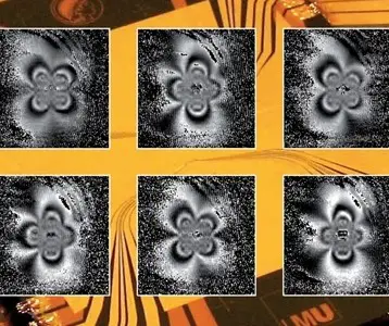
In their paper, the researchers write that the strain produced small, raised triangular graphene bubbles 4 to 10 nanometers across in which the electrons occupy discrete energy levels rather than the broad, continuous range of energies allowed by the band structure of unstrained graphene. By scanning tunneling microscopy, they discovered this new electronic behavior, which led them to believe that these so-called Landau levels are reminiscent of the quantized energy levels of electrons in the simple Bohr model of the atom.
This recent study represents a worldwide effort in trying to understand better the attributes and properties of graphene; only in the last year a European team predicted what they termed a pseudo quantum Hall effect in strained graphene – and Crommie’s research group observed this very quantization through their experiments. Boston University physicist Antonio Castro Neto, who was visiting Crommie’s laboratory at the time of the discovery, immediately recognized the implications of the data, and subsequent experiments confirmed that it reflected the pseudo quantum Hall effect predicted earlier.
When asked about external interferences, Crommie said that they experimented with thermal noise, and it would not interfere with the effect in graphene – even at room temperature, since "pseudomagnetic fields" inside the nanobubbles are very high. In fact, the energy levels are separated by hundreds of millivolts, much higher than room temperature. However, nanobubble experiments performed in Crommie’s laboratory were performed at very low temperatures.
Crommie does not conceal his enthusiasm. “What is so exciting now is that we have data that shows these ideas are not so crazy; the observation of these giant pseudomagnetic fields opens the door to room-temperature ‘straintronics,’” he said. “The idea is to use mechanical deformations in graphene to engineer its behavior for different electronic device applications."
TFOT has also covered an innovative method used to see graphene, researched at Northwestern University, research of superconductivity using magnets, conducted at Los Alamos National Laboratory, and the discovery of the illogical secret of superconductors, made by researchers from Princeton University.
For more information about the graphene research conducted at the UC Berkeley, see the university’s press release.