|
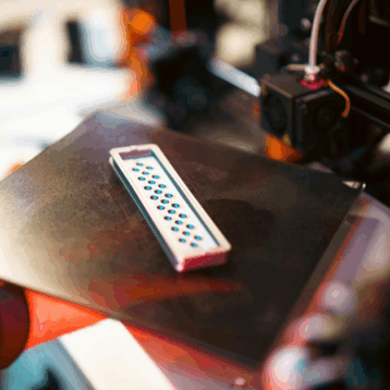
Stanford’s new expandable chips are composed of nano-scale, floating ‘islands’ of silicon, which are surrounded by silicon coils. Each such ‘island’ can be separately altered to include transistors, sensors, or materials for miniature solar cells. When the corners of the chip are pulled on, the coils of silicon wire unwind around the silicon ‘islands’, which in turn spread apart to form a net-like array of silicon devices. Peter Peumans, Professor of Electrical Engineering at Stanford University and lead researcher on the project, said that using optimal laboratory equipment it will be possible to manufacture chips capable of expanding to cover an area thousands and even tens of thousands larger than their original size. He also added that one of the main challenges faced by his team was the task of showing that the coils around the silicon “islands” would be strong enough not to break as they unwind and stretch the material.
The semiconductor industry has long been focused on the problem of packing the maximal amount of transistors into the minimal amount of space, striving to lower the products’ costs. However, experts say many modern applications require more distributed transistors and other silicon-based devices than those produced today. Stanford’s new chip design has a broad range of potential applications. For example, the upcoming generation of a high standard, energy efficient displays (such as organic LED or OLED displays) require higher performance transistors, which are normally produced using extremely expensive high quality silicon. Peumans’s method not only minimizes the amount of silicon that is used, but also produces pre-wired devices, dramatically decreasing production costs.
|
The expandable chips could also be used to build cheaper solar panels that will require much less silicon to be completely coated, still maximally absorbing the sunlight. In early 2007, Peumans founded the “NetCrystal” company, which will manufacture such solar panels. Peumans estimates that these solar panels will cost about a third of the price of the solar panels on the market today. Stanford researchers are also working with Boeing on integrating this technology into aircraft sensor networks. Silicon-based sensors will be implanted between the composite material layers, which constitute various parts of the aircraft, such as the wings. These sensors will then be used to monitor the material condition, detecting cracks and other flaws.
TFOT recently covered a research project conducted by a team from the Sandia National Laboratories. The team developed new sensors that can detect structural defects in aircrafts and in structures.
Peumans and his team are currently working on developing devices that will demonstrate the expandable chips’ functionality – they have already succeeded in building a prototype solar cell and several other applications are “in production”.
TFOT recently covered another cheap process for printing transistors developed by the American company “Kovio”. You can also have a look at some programmable bending polymers, which were developed at the Hebrew University in Jerusalem, Israel.


