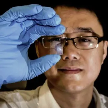
The needle, made by Moh’d Rezeq in the group lead by Professor Robert Wolkow at the University of Alberta and the National Institute for Nanotechnology, was initially much blunter. The needle was exposed to pure nitrogen atmosphere which made it thinner and thinner. Tungsten is chemically highly reactive and the nitrogen is used to roughen the tungsten surface. But at the tip, where the electric field created by applying a voltage to the tungsten is at its maximum, N2 molecules are driven away. This process reaches an equilibrium condition in which the point is very sharp.
Furthermore, what N2 is present near the tip helps to stabilize the tungsten against further chemical degradation. Indeed, the resultant needle is stable up to temperatures of 900 degrees Celsius even after 24 hours of exposure to air.
The probe tips used in scanning tunneling microscopes (STMs), even though they produce atomic-resolution pictures of atoms sitting on the top layer of a solid material, are not themselves atomically thin. Rather their radius of curvature at the bottom is typically 10 nm or more.
According to Wolkow says that although a narrower tip will be useful in the construction of STM arrays (you can pack more tips into a small area; and a wide array might even permit movies of atomic motions) the spatial resolution won’t improve thereby. The real benefit of the sharp tungsten tips, he believes, will be as superb electron emitters. Being so slender, they would emit electrons in a bright, narrow, stable stream.
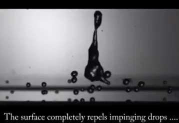
The picture shows a field ion microscope (FIM) image of a very sharp tungsten needle. The small round features on the image are individual atoms. The lighter colored elongated features are traces captured as atoms moved during the imaging process (approximately 1 second).


