As electronic devices become smaller, faster, and more flexible, traditional materials used in circuit design are struggling to keep pace. This is where nanopaste comes in—a groundbreaking material that offers unique advantages for modern electronics. With its ability to form ultra-thin conductive layers and adapt to various substrates, nanopaste is becoming increasingly important in the development of advanced circuit designs. This essay explores what nanopaste is, its manufacturing benefits, and the diverse applications it is enabling in the field of electronics.
Nanopaste – What is it?
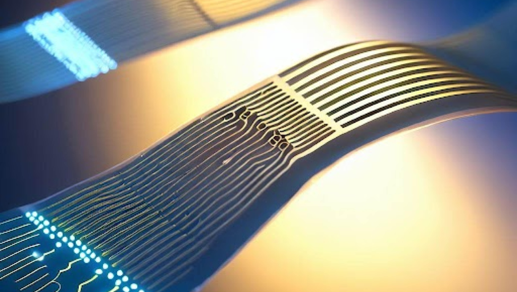
Nanopaste is a highly specialized material made of nanoparticles suspended in a solvent or paste, specifically designed for use in electronic circuits. These nanoparticles are often composed of conductive metals such as silver or copper, which give the paste its remarkable electrical properties. Unlike traditional conductive materials like copper wiring or printed circuit board (PCB) traces, nanopaste allows for much finer, more precise applications. Its ability to form ultra-thin, flexible layers distinguishes it from older technologies that tend to be bulkier and less adaptable to the increasingly compact design needs of modern electronics.
One of the key reasons nanopaste stands out is its enhanced electrical conductivity, which is superior to many conventional materials. This makes it particularly useful in circuits that require high-performance electrical connections in tight spaces. Additionally, its flexibility allows it to be applied to a wide range of surfaces, including flexible substrates used in wearable technology. Its unique properties make it an ideal solution for the future of electronics, where flexibility, miniaturization, and performance are all critical factors.
The Manufacturing Marvels of Nanopaste
The manufacturing process for nanopaste is one of its key advantages, as it allows for highly advanced printing techniques. Nanopaste can be applied using methods such as inkjet printing or aerosol jet printing, both of which enable precise control over the deposition of the material. These techniques allow manufacturers to apply nanopaste in very fine layers, essential for creating the high-density circuits required in devices like smartphones and other compact electronics.
After nanopaste is applied to a substrate, a process called sintering follows. Sintering involves heating the nanopaste to bond the nanoparticles together without damaging the underlying materials. What sets nanopaste apart from traditional methods is that the sintering process occurs at much lower temperatures than are required for conventional soldering or printing techniques. This reduces the risk of damaging sensitive components and substrates during the manufacturing process, making it more compatible with flexible materials used in emerging technologies.
Nanopaste offers several advantages over traditional methods. Because it requires lower temperatures for sintering, it consumes less energy, resulting in cost savings and a lower environmental impact. It also generates less waste, as the precise application techniques minimize the amount of material used. Additionally, nanopaste can be applied to a wide range of substrates, including flexible ones, which opens up new possibilities for device design.
Diverse Applications of Nanopaste in Electronics
One of the most exciting applications of nanopaste is in wearable technology. The flexible nature of nanopaste allows it to be used in electronics that need to bend and stretch, such as fitness trackers or smartwatches. In these devices, nanopaste provides durable, flexible connections that withstand the wear and tear of everyday use. Its ability to form ultra-thin conductive layers means that electronic components can be seamlessly integrated into fabrics or other soft materials, making wearables more comfortable and less obtrusive.
Nanopaste is also making a significant impact in high-density circuitry. The fine resolution achievable with nanopaste makes it ideal for the compact circuit designs found in smartphones and other devices that require high performance in small packages. By enabling tighter, more efficient circuit layouts, nanopaste is helping to push the limits of what is possible in miniaturized electronics.
In addition to these established uses, nanopaste holds great promise for future technologies. Emerging fields like bioelectronics and photovoltaics are exploring the potential of nanopaste for creating flexible, highly efficient circuits that could revolutionize everything from medical devices to solar energy systems. While these applications are still in development, nanopaste’s unique properties make it an attractive material for cutting-edge research and innovation.
Conclusion
Nanopaste is proving to be a game-changer in circuit design, offering enhanced conductivity, flexibility, and manufacturing efficiency. Its ability to be applied with advanced printing techniques and its compatibility with a wide range of substrates make it ideal for both current and future electronics. From wearable devices to high-density circuit boards, nanopaste is shaping the future of how we build electronic systems, allowing for more compact, efficient, and adaptable designs. As research continues, its role in emerging technologies will likely expand, further cementing its importance in the field of electronics.