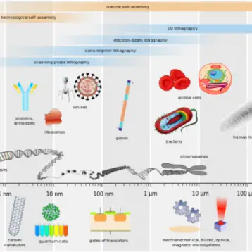
Microscopic in size, these complex 3-D nanostructures have been extremely difficult to assemble and fabricate. Using the new procedure, combining the approaches of engineering technology and chemistry, previous limitations have been shattered. Through phase-shift lithography and the chemical model of self-assembly of colloidal nanoparticles, researchers have been able to produce 3D nanostructured materials that feature grooves, shapes, and formations measuring just billionths of a millimeter.
Phase-shift lithography is a technique of masking to shape the intensity of light shining on semi-conductor wafers. By taking advantage of the behavior of light in the near-field region (a distance less than the wavelength of light), it can produce features down to around 500 nanometers. By allowing the engineered particles to assemble themselves into energetically favorable close-packed arrangements, the need for construction on this small scale is unnecessary.
The team of scholars and nanotech experts at the MIT whose expertise is in optics, are planning to manufacture photonic crystals through this technology. Their methods make it possible to create many tiny 3-D devices like filters and drug transporters for biomedical purposes, phononic devices that can alter and control heat and sound waves, and microscopic high-tech mechanisms.
The main thing that makes this nanofabrication procedure special is its simplicity and amazingly accurate results. John Rogers, a professor of materials science and engineering and professor of chemistry at the University of Illinois at Urbana-Champaign commented on this technology saying, “The experimental simplicity, and the resulting access to structures that would be difficult or impossible to achieve in other ways, suggest that the approach will be useful for many fields of application in the future.”
TFOT has covered nanotechnology in its various forms in articles such as “NASA’s Super Cooling Technology,” “Nanoscale Transistors Probe Cells,” and “Pushing Ions Through Carbon Nanotubes.” Also, read more about MIT’s NanoStructures Laboratory here.