|
Unlike flash memory, where bits are stored as an electronic charge (presence of charge at a particular spot on the chip translates to the binary ‘1’, and a lack of charge is represented by ‘0’), PMC memory uses nanowires from copper atoms to record binary data. In order to write ‘1’, it builds an on-demand copper bridge between two electrodes and interprets the absence of a wire as the binary ‘0’. “In using readily available materials [such as copper], we’ve provided a way for this memory to be made at essentially zero extra cost, because the materials you need are already used in the chips – all you have to do is mix them in a slightly different way,” says Michael Kozicki, Director of CANi.
Over the past years, the race towards more memory in less space has gained speed due to continuous demands for decrease in size of consumer electronics products. While the scientists are trying to refine existing technologies, they are also considering new approaches, such as optical and laser-based storage systems. ASU scientists, who conducted their research in collaboration with Research Center Juelich in Germany, focused on both aspects of the problem; The researchers aimed to improve performance by using special materials while also switching from charge-based storage to resistance-based storage technology. “We’ve developed a new type of old memory, but really it is the perfect memory for what’s going to be required in future generations,” Kozicki says. “It’s very low-energy. You can scale it down to the nanoscale. You can pack a lot of it into a small space.”
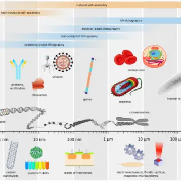
The new technology relies on the field of nanoionics – the study of processes connected with fast ion transport in nanoscale systems. The system moves the charged particles (ions) themselves, instead of the electrons among them, and the researchers say this provides a great advantage. “We’ve actually been able to move something the size of a virus between electrodes to switch them from a high resistance to a low resistance, which is great for memory,” Kozicki says.
While this technology is still under development, CANi has already licensed the concept for high-performance resistance-change memory to three companies, including Micron Technology and Quimonda. The scientists say that the real innovation of their technology is in the discovery of a new way to use materials already in use for chip manufacturing in the semiconductor industry, such as mixing copper in silicon dioxide – a technique previously avoided by manufacturers. “People have actually gone to great lengths to keep the silicon oxide and the copper apart,” Kozicki says. “But in our case, we are very interested in mixing the copper with the oxide – basically, so that it would become mobile and move around in the material. Because it can move in there, we can make a sort of nanoscale switch. This very, very small switch can be used in memory applications, storing information via a range of resistance values.”
The researchers believe this new type of memory could be a natural fit for various products, due to its high power efficiency, which allows a lot of memory to be packed in the device without draining battery power.
TFOT has previously covered several novel memory storage technologies including Samsung’s hybrid and solid state hard drives, Freescale’s MRAM memory, Brown University’s nanowires based storage and Nanosy’s improved flash memory technology.
You can find more information on this new storage system here.


