|
")
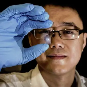
The team leader, CU-Boulder Assistant Professor Robert McLeod, explained that highly concentrated beams of blue light were manipulated to create lines that are thousands of times narrower than human hair. The researchers then succeeded to trim the edges of the inscribed patterns by using a halo of ultraviolet (UV) light. “We are essentially drawing a line with a marker on a nanotechnology scale and then erasing its edges,” said McLeod.
In their project, the researchers first used a tabletop laser to direct highly focused beams of observable blue light onto liquid molecules identified as monomers. This subsequently instigated a chemical reaction that bonded the monomers into a plastic-like polymer solid. By moving a single beam through the material, a tiny line would appear inscribed upon the surface.
A second ultraviolet light was then set up to shine around the focused blue light as a halo, with the blue light concentrated in its middle. The UV halo essentially blocked the chemical reaction occurring along the edges of the line, thus preventing the edges from developing. The result of this approach was a much finer formation than those previously achieved in the field.
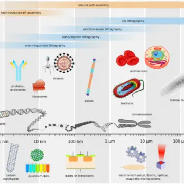
The new method presents novel opportunities in the race towards further reducing the size of transistor circuitry – a process predominately driven by the global electronic market, which continuously aims for smaller and more powerful microchips. “We now have a set of new tools. We believe this is a new way to do nanotechnology” – said McLeod. He further added that this new finding could lead the way to the development of more effective nanotechnology devices including “nanomotors.”
TFOT has previously written about the world’s smallest transistor developed by carving graphene into tiny electronic circuits with individual transistors not much larger in size than a molecule. We have also covered a technique to print electronics using a new silver-based ink that enables the production of flexible, stretchable, and spanning microelectrodes that transmit signals from one circuit element to another. You are also welcome to read about novel nanomotors that are up to 10 times more powerful than existing motors.
Additional information on this CU-Boulder research can be obtained at University of Colorado’s website.
Image icon credit: Kunal Mukherjee