|
")
The switching device enables pulses to be directed within a network and thus efficiently transverse between different processor cores on the chip. “This new development is a critical addition in the quest to build an on-chip optical network,” says Yurii Vlasov, Manager of Silicon Nanophotonics at IBM’s TJ Watson Research Center. “In view of all the progress that this field has seen for the last few years, it looks that our vision for on-chip optical networks is becoming more and more realistic”.
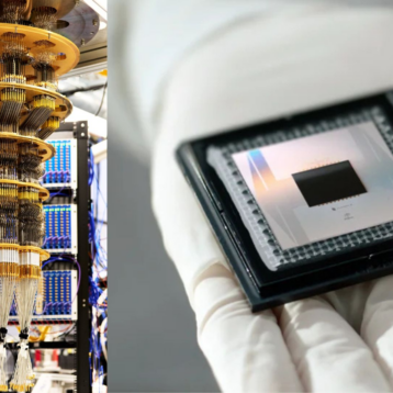
IBM’s silicon broadband optical switch is an integral component in enabling on-chip optical interconnections. Drawing on the existing electrical signals available in the chip, the switching device performs the key role of “directing traffic” within the network by converting these electrical signals to light pulses. Subsequently, the switch devices are set into the necessary positions, and the optical messages are routed from the transmitting core to the receiving core.
The IBM team was able to show that the switch has advantages for on-chip applications. Firstly, the switch is incredibly compact. This complies with integration requirements for future multi-core processors. As many as 2,000 switches are able to be mounted densely in an area of one square millimeter.
|
")
To add to this incredible space saving characteristic, the device is capable of transmitting data of high bandwidths. A bandwidth of light holds a multitude of different colors, which are scientifically distinctive wavelengths. Data can then be transmitted through every individual light wavelength. Seeing as one wavelength is able to carry data at up to 40 Gb/s, the switch can supply a bandwidth exceeding 1 Tb/s. To fully exploit this fantastic attribute, the switching device should be utilized in methods for routing large messages between distant cores.
The most novel aspect of the finding is that the IBM team has demonstrated for the first time that their device functions within a realistic on-chip environment. Depending on the manner in which the processors function, temperature “hot-spots” may invariantly cause the temperature of the chip to alter dramatically in different areas. The results show that the switching device is able to tolerate these temperature-drifts. This represents a most critical requirement for on-chip optical networks.
As the users’ demand continues to grow, chip manufacturers race towards increasing parallelism in computation by multi-threading. This increases the number of cores on a single chip by building large scale multi-chip systems. Currently, the IBM Cell Processor, which powers Sony’s PlayStation 3 gaming console, consists of nine “brains,” or cores (capable of a combined theoretical bandwidth of just over 200 GB/s), on a single chip. The optical switching device is expected to revolutionize the speed of the next generation of processors.
Today, the individual cores located on multi-core microprocessors communicate with one another over millions of tiny copper wires. At the estimated performance level of the optical switching device, the copper wiring would simply use up too much power and would be incapable of transmitting the enormous amount of information required in multi-core processors.
IBM researches are exploring an alternative solution to the problem associated with copper wires by connecting cores using pulses of light in an on-chip optical network based on silicon nanophotonic integrated circuits. Like a long-haul fiber-optic network, this miniature on-chip network will transmit, receive, and route messages encoded in light pulses, between individual cores. It is estimated that using light instead of wires will enable transmitting 100 times more information between cores, while using 10 times less power, and consequently, generating less heat.
The idea is that each core will receive and transmit large amounts of data between the other processor cores on the chip simultaneously. Like all products on the market, IBM is expected to have stiff competition from other large scale chip manufacturers such as Intel, who in March 2008, discussed cutting edge microprocessors and technologies including the next generation “Tukwila”.
|
")
Tukwila is Intel’s next-generation Itanium processor with four cores, a 30MB total cache, QuickPath Interconnect, dual Integrated Memory Controller, and mainframe-class RAS features. It is the world’s first 2 billion transistor microprocessor and is projected to deliver more than double the performance of the current generation Itanium processors. Tukwila is targeted for production towards the end of 2008.
With Tukwila looming on the horizon, IBM needs to develop their silicon broadband optical switch to a commercial level, if they want to keep up with their competitors.
TFOT has also covered other ‘nano’ related topics, such as the use of nano-diamonds in quantum computing by scientists at the University of Melbourne, who used the diamonds’ properties in an attempt to create quantum computers capable of performing parallel computing tasks. TFOT also reported on a new nanoscale technology for memory storage developed by researchers at Arizona State University (ASU). The researchers used a new type of computer memory called ‘programmable metallization cell’ (PMC), which is low-cost and more power-efficient than conventional memory storage systems.
Additional information on this development and on the IBM’s nanophotonics project can be found on IBM’s website (and more here).